- 您现在的位置:买卖IC网 > Sheet目录493 > NTTFS5826NLTWG (ON Semiconductor)MOSFET PWR N-CH 60V 20A 8-WDFN
�� �
�
�NTTFS5826NL�
�Power� MOSFET�
�60� V,� 24� m� W� ,� Single� N� ?� Channel,� m� 8FL�
�Features�
�?� Small� Footprint� (3.3� x� 3.3� mm)� for� Compact� Designs�
�?� Low� Q� G(TOT)� to� Minimize� Switching� Losses�
�?� Low� Capacitance� to� Minimize� Driver� Losses�
�?� These� are� Pb� ?� Free� Devices�
�http://onsemi.com�
�Applications�
�?� Motor� Drivers�
�?� DC� ?� DC� Converters�
�?� Synchronous� Rectification�
�?� Power� Management�
�MAXIMUM� RATINGS� (T� J� =� 25� °� C� unless� otherwise� noted)�
�V� (BR)DSS�
�60� V�
�R� DS(on)� MAX�
�24� m� W� @� 10� V�
�32� m� W� @� 4.5� V�
�N� ?� Channel�
�D�
�I� D� MAX�
�20� A�
�Parameter�
�Drain� ?� to� ?� Source� Voltage�
�Symbol�
�V� DSS�
�Value�
�60�
�Unit�
�V�
�Gate� ?� to� ?� Source� Voltage�
�V� GS�
�"� 20�
�V�
�G�
�Continuous� Drain�
�Current� R� Y� J� ?� mb�
�(Notes� 1,� 2,� and� 3)�
�T� mb� =� 25� °� C�
�T� mb� =� 100� °� C�
�I� D�
�20�
�14�
�A�
�S�
�T� A� =� 25� °� C�
�Power� Dissipation�
�R� Y� J� ?� mb� (Notes� 1,� 2,�
�and� 3)�
�Continuous� Drain�
�Current� R� q� JA� (Notes� 1�
�&� 3)�
�Power� Dissipation�
�R� q� JA� (Notes� 1� &� 3)�
�Pulsed� Drain� Current�
�T� mb� =� 25� °� C�
�Steady� T� mb� =� 100� °� C�
�State�
�T� A� =� 100� °� C�
�T� A� =� 25� °� C�
�T� A� =� 100� °� C�
�T� A� =� 25� °� C,� t� p� =� 10� m� s�
�P� D�
�I� D�
�P� D�
�I� DM�
�19�
�10�
�8�
�6�
�3.1�
�1.6�
�133�
�W�
�A�
�W�
�A�
�1�
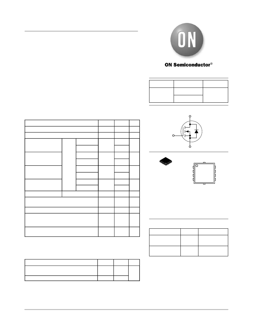
�WDFN8�
�(� m� 8FL)�
�CASE� 511AB�
�5826�
�A�
�MARKING� DIAGRAM�
�1�
�S� D�
�S� 5826� D�
�S� AYWW� G� D�
�G� G� D�
�=� Specific� Device� Code�
�=� Assembly� Location�
�Operating� Junction� and� Storage� Temperature�
�Source� Current� (Body� Diode)�
�Single� Pulse� Drain� ?� to� ?� Source� Avalanche�
�Energy� (T� J� =� 25� °� C,� V� DD� =� 50� V,� V� GS� =� 10� V,�
�I� L(pk)� =� 14.4� A,� L� =� 1.0� mH,� R� G� =� 25� W� )�
�Lead� Temperature� for� Soldering� Purposes�
�(1/8� ″� from� case� for� 10� s)�
�T� J� ,� T� stg�
�I� S�
�E� AS�
�T� L�
�?� 55� to�
�175�
�20�
�20�
�260�
�°� C�
�A�
�mJ�
�°� C�
�Y� =� Year�
�WW� =� Work� Week�
�G� =� Pb� ?� Free� Package�
�(Note:� Microdot� may� be� in� either� location)�
�ORDERING� INFORMATION�
�Device� Package� Shipping� ?�
�Stresses� exceeding� Maximum� Ratings� may� damage� the� device.� Maximum�
�Ratings� are� stress� ratings� only.� Functional� operation� above� the� Recommended�
�Operating� Conditions� is� not� implied.� Extended� exposure� to� stresses� above� the�
�Recommended� Operating� Conditions� may� affect� device� reliability.�
�THERMAL� RESISTANCE� MAXIMUM� RATINGS�
�Parameter� Symbol� Value� Unit�
�Junction� ?� to� ?� Mounting� Board� (top)� ?� Steady� R� Y� J� ?� mb� 7.9� °� C/W�
�State� (Notes� 2,� 3)�
�NTTFS5826NLTAG� WDFN8� 1500/Tape� &� Reel�
�(Pb� ?� Free)�
�NTTFS5826NLTWG� WDFN8� 5000/Tape� &� Reel�
�(Pb� ?� Free)�
�?For� information� on� tape� and� reel� specifications,�
�including� part� orientation� and� tape� sizes,� please�
�refer� to� our� Tape� and� Reel� Packaging� Specification�
�Brochure,� BRD8011/D.�
�Junction� ?� to� ?� Ambient� ?� Steady� State� (Note� 3)�
�R� q� JA�
�48�
�1.� The� entire� application� environment� impacts� the� thermal� resistance� values� shown,�
�they� are� not� constants� and� are� only� valid� for� the� particular� conditions� noted.�
�2.� Psi� (� Y� )� is� used� as� required� per� JESD51� ?� 12� for� packages� in� which�
�substantially� less� than� 100%� of� the� heat� flows� to� single� case� surface.�
�3.� Surface� ?� mounted� on� FR4� board� using� a� 650� mm� 2� ,� 2� oz.� Cu� pad.�
�?� Semiconductor� Components� Industries,� LLC,� 2011�
�November,� 2011� ?� Rev.� 2�
�1�
�Publication� Order� Number:�
�NTTFS5826NL/D�
�发布紧急采购,3分钟左右您将得到回复。
相关PDF资料
NTTS2P02R2
MOSFET P-CH 20V 2.4A 8MICRO
NTTS2P03R2
MOSFET P-CH 30V 2.1A 8MICRO
NTUD3127CT5G
MOSFET N/P-CH 20V SOT-963
NTUD3128NT5G
MOSFET N-CH DUAL 20V SOT-963
NTUD3129PT5G
MOSFET P-CH DUAL 20V SOT-963
NTUD3169CZT5G
MOSFET N/P-CH 20V SOT-963
NTUD3170NZT5G
MOSFET N-CH DUAL 20V SOT-963
NTUD3171PZT5G
MOSFET P-CH DUAL 20V SOT-963
相关代理商/技术参数
NTTFSC4821NTAG
功能描述:IGBT 晶体管 NFETU8FL 30V 57A 10.8M Ohm
RoHS:否 制造商:Fairchild Semiconductor 配置: 集电极—发射极最大电压 VCEO:650 V 集电极—射极饱和电压:2.3 V 栅极/发射极最大电压:20 V 在25 C的连续集电极电流:150 A 栅极—射极漏泄电流:400 nA 功率耗散:187 W 最大工作温度: 封装 / 箱体:TO-247 封装:Tube
NTTFSC4823NTAG
功能描述:IGBT 晶体管 NFETU8FL 30V 50A 17.5MOHM
RoHS:否 制造商:Fairchild Semiconductor 配置: 集电极—发射极最大电压 VCEO:650 V 集电极—射极饱和电压:2.3 V 栅极/发射极最大电压:20 V 在25 C的连续集电极电流:150 A 栅极—射极漏泄电流:400 nA 功率耗散:187 W 最大工作温度: 封装 / 箱体:TO-247 封装:Tube
NTTS2P02R2
功能描述:MOSFET 20V 2.4A P-Channel RoHS:否 制造商:STMicroelectronics 晶体管极性:N-Channel 汲极/源极击穿电压:650 V 闸/源击穿电压:25 V 漏极连续电流:130 A 电阻汲极/源极 RDS(导通):0.014 Ohms 配置:Single 最大工作温度: 安装风格:Through Hole 封装 / 箱体:Max247 封装:Tube
NTTS2P02R2/D
制造商:未知厂家 制造商全称:未知厂家 功能描述:Power MOSFET -2.4 Amps, -20 Volts
NTTS2P02R2_06
制造商:ONSEMI 制造商全称:ON Semiconductor 功能描述:Power MOSFET -2.4 Amps, -20 Volts
NTTS2P02R2G
功能描述:MOSFET 20V 2.4A P-Channel RoHS:否 制造商:STMicroelectronics 晶体管极性:N-Channel 汲极/源极击穿电压:650 V 闸/源击穿电压:25 V 漏极连续电流:130 A 电阻汲极/源极 RDS(导通):0.014 Ohms 配置:Single 最大工作温度: 安装风格:Through Hole 封装 / 箱体:Max247 封装:Tube
NTTS2P03R2
功能描述:MOSFET -30V -2.48A RoHS:否 制造商:STMicroelectronics 晶体管极性:N-Channel 汲极/源极击穿电压:650 V 闸/源击穿电压:25 V 漏极连续电流:130 A 电阻汲极/源极 RDS(导通):0.014 Ohms 配置:Single 最大工作温度: 安装风格:Through Hole 封装 / 箱体:Max247 封装:Tube
NTTS2P03R2/D
制造商:未知厂家 制造商全称:未知厂家 功能描述:Power MOSFET -2.48 Amps, -30 Volts